Intel, AMD and other industry heavyweights are creating a new chiplet standard
Some of the biggest processor manufacturers, including Intel, AMD, Qualcomm, Arm, TSMC, and Samsung, are teaming up to define a new standard for chip-based processors. The new standard, called Universal Chiplet Interconnect Express (UCIe for short), aims to define an open, interoperable standard for combining multiple silicon dies (or chiplets) into a single package.
Intel, AMD, and others are already developing or selling chiplet-based processors in one form or another — most AMD Ryzen processors use chiplets, and future Intel Sapphire Rapids Xeon processors will, too. But all of these chips use different interconnects to enable communication between the chiplets. The UCIe standard, if it succeeds, will replace them with a single standard, theoretically making it easier for small companies to use chipsets or use another company’s chips in their own products.
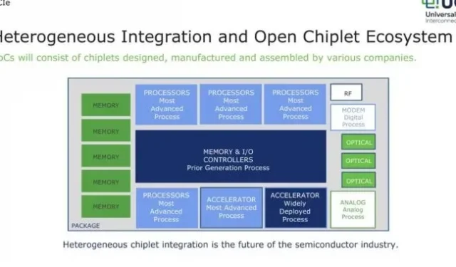
Chip-based designs are beneficial for large chip fabrication at advanced manufacturing sites, in part because they reduce the amount of silicon that manufacturers have to waste. If a manufacturing defect affects one CPU core, throwing away (or removing) one 8-core chiplet is much cheaper than throwing away a huge 16- or 32-core CPU die. Chip designs also allow the combination of chips and manufacturing processes. For example, you can use an older, cheaper process for your chipset and a newer, more advanced process for processor cores and caches. Or you can put an AMD GPU in the same case as an Intel processor.
According to AnandTech, the UCIe standard will cover the physical and protocol layers of chip design. The standard will define how chiplets should be connected to each other and a protocol to facilitate communication between chiplets. But chip designers will be free to package these chiplets however they see fit, allowing the chiplets to communicate with each other directly through the package substrate or using some kind of silicon-based bridge or other intermediary.
To account for these different physical packaging options, UCIe version 1.0 defines two different levels of performance. The “Standard”package requires 16 data lanes and up to 25mm of space between chipsets, while the “Extended”package uses 64 data lanes and only allows 2mm space.
The protocols underlying UCIe are PCI Express and the related Compute Express Link (CXL) standards, which are well known to chip manufacturers. But companies that have already developed more advanced or dedicated protocols for communication between chipsets, such as AMD and its Infinity Fabric, will be able to use these protocols while remaining UCIe compliant. UCIe was originally developed by Intel and then donated to the wider UCIe group to serve as the basis for a new standard. But the group’s member companies “will start working together on next-generation UCIe technology”starting later this year.
If you need more technical details about the UCIe standard, you can find the white paper here.
Image listing from AMD
Leave a Reply